What IBM’s new AI-enabling, brain-inspired computer chips could mean for DOD
Technologists at the Air Force Research Lab, Sandia National Laboratory and other government research hubs are developing real-world use cases to inform the maturation of a new IBM-produced computer chip prototype — with a cutting-edge, brain-inspired architecture — that holds potential to drastically innovate where and how the military can harness the power of artificial intelligence, DefenseScoop has learned.
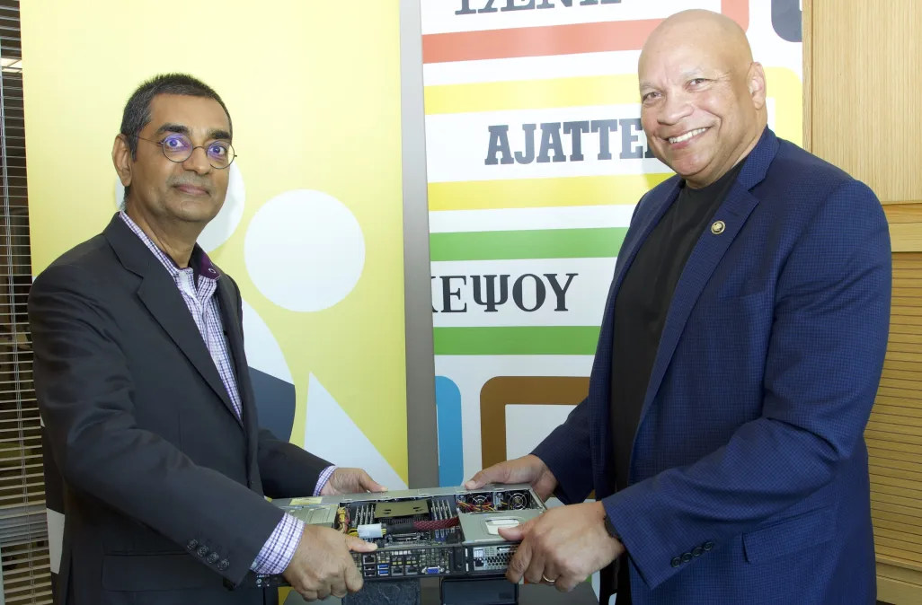
As soon as they were approached about funding the in-the-works chip and IBM’s underpinning NorthPole project in 2021, Assistant Secretary of Defense for Critical Technologies Maynard Holliday and his team immediately “recognized the utility and potential — I don’t want to say revolutionary, but game-changing, leap-ahead capability that this represented,” he said in an interview on Wednesday.
Dharmendra Modha, IBM Research’s NorthPole lead, has been working on what would evolve into NorthPole since around 2004. On Thursday, he published results of his team’s research in Science, arguing that this new AI-enabling semiconductor prototype has proven to outperform all the latest prevalent chip architectures on the market, including the most advanced.
A major element of its promise is that all the memory for the device is stored directly on the chip — as opposed to elsewhere, like the cloud or company-owned servers.
“I would say NorthPole is the faint reflection of the brain in the middle of a silicon wafer that points to a new direction in computer architecture … What that means, the world and we will together figure it out over the years to come,” Modha noted.
In separate interviews on Wednesday, IBM’s Modha and DOD’s Holliday briefed DefenseScoop on the making and uniqueness of this new prototype, and where the U.S. military and defense researchers might take it from here.
“What this enables is that compute to be able to be done at the point of interaction. And so you can think about how that’s really valuable for the soldier and/or the platform when you’re in a GPS-[strained] or contested electromagnetic environment and the compute is being able to be done locally,” Holliday said.
‘Just scratching the surface’
According to Modha, the phrase “‘the architecture of the brain’” refers to how the organ stores, moves and schedules information. And “‘technology of Mother Nature,’” he explained, encompasses how the chemicals and the organic substrate of the brain implement that architecture.
“What we have taken is the architecture of the brain — the blueprint of how it computes, how it stores, how it connects, how it schedules, how it communicates and how it interacts with the world — those principles, we have extracted and implemented in an off-the-shelf silicon technology process. So it does not have any of the organic technologies of the brain, such as the chemical signaling, or anything like that. It’s taking the architecture and implementing it in today’s technology — that’s the essence of the innovation,” Modha told DefenseScoop.
One of the government’s top engineering and robotics experts and technology innovation leaders, Holliday has helped push forward a range of crucial national security-aligned capabilities.
“This always blows my mind when I think of it. So, our brains have 10 to the 14th or 100 trillion synapses, and we have [billions of] neurons. Humans have created civilization, and our brain consumes the power of a light bulb, right? And it occupies the volume of a large soda bottle. So, you know, it’s amazing,” he said.
Modha “is right about this being a slight reflection of the brain,” Holliday added, in that the architectures are in many ways similar. However, the NorthPole prototype chip currently has 22 billion transistors — compared to the billions or trillions of synapses in human brains.
“We’re just scratching the surface with respect to architecture. But nature is, a lot of times, the best guide for … what works, because we’re still alive and thriving with our brain architecture. And so, to the extent that we can mimic that in machinery, it’s showing that it’s as powerful or more powerful than this von Neumann architecture — which is memory and central processing [unit]-separate. And you have this classic, what we call ‘von Neumann’ bottleneck — is a testament to how efficient a neuromorphic architecture is,” Holliday told DefenseScoop.
Today’s computer architecture is still largely dominated by what’s known as the von Neumann architecture, Modha explained. That term has roots that trace back to around 1945 from a description by John von Neumann, a leading defense scientist and mathematician who notably worked on the Manhattan Project to build the world’s first atomic bombs. In such architectures, memory and CPUs that process information are separated. The von Neumann bottleneck refers to the phenomenon where the time and power it takes to shuffle data between memory, processing, and any other devices within a chip can limit or affect how the corresponding system performs.
The NorthPole prototype is designed to set a completely different path from the von Neumann architecture by combining features in one place. And that also enables the nascent chip to carry out AI inferencing — or the process of running through a deep learning network’s data in real time on an application — considerably faster than others that are out there currently.
“If you look at any computer chip, broadly, it has five dimensions: computation, memory, communication, control and input-output. Along all these five dimensions, NorthPole breaks with the past,” Modha said.
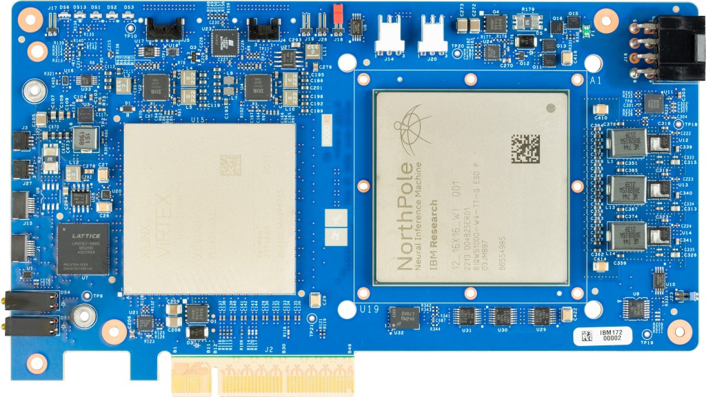
NorthPole was fabricated with a 12-nm node process. According to Modha’s new research published in Science, his team tested the prototype using the ResNet-50 model, the well-known convolutional neural net for image recognition that benchmarks the performance of AI chips.
The researchers found that NorthPole can recognize images faster and is 25 times more energy efficient when it comes to the number of frames interpreted per joule of power required, than common 12-nm GPUs and 14-nm CPUs like those now widely used and made by Nvidia and other major players.
It also out-performed competitors in space and time efficiency.
Pointing to those results and why they matter for the defense enterprise, Holliday spotlighted NorthPole’s power to ingest multiple sensor modalities including audio, electro-optical, infrared and sonar signals; wide-area motion imagery; synthetic aperture radar, and Lidar.
Autonomous vehicles can use Lidar to characterize everything in their ambient environments, he noted, and electro-optical and infrared sensors can essentially use heat signatures to classify helicopters and other platforms.
“You can think about acoustic sensors that could be on a dismounted soldier or on a platform, being able to discern audio feedback from targets or just to discern, you know, signatures of weapons fires. So then you can say, ‘Alright, well, that’s, you know, this kind of weapon or that kind of weapon being fired’ … because you know what the audio signature is,” Holliday said.
“The important thing to note is it’s low, what we call ‘SWAP— size, weight and power,” he added regarding the AI chip prototype.
His hope is that such systems could potentially last longer, have longer endurance, and be more densely configured to provide more compute power.
“You can think about it on the dismounted soldier, on the [unmanned aerial vehicle], or on the [unmanned underwater vehicle]. So, all of these platforms where we want to exploit man-machine teaming, where we want to do swarming. To be able to, again, have compute at the tactical edge — that makes all of these systems smarter and more capable,” Holliday told DefenseScoop.
Next moves
Modha has been working to generate the prototype that NorthPole has become since the early 2000s for IBM, with support from the Defense Advanced Research Projects Agency, the Air Force and others along the way.
When Holliday returned to the Pentagon in 2021 to serve in his latest post, he and his team were approached about funding IBM’s NorthPole pursuit. “Unfortunately, it had been canceled by the previous administration,” he told DefenseScoop.
“They came to me to say, ‘We are close. This is a capability we absolutely need — because it provides AI compute at the edge,’” Holliday recalled. The Office of the Secretary of Defense then opted to fund them to finish the job so that the chips could be fabricated in low numbers in the U.S. and be tested and evaluated by the government and the industrial base.
Now, that’s happening across federal, defense and other research organizations.
Each prototype AI chip has to be placed on a field programmable array to then be integrated to work within more complex systems.
Looking to ultimately operationalize the prototype, Holliday confirmed that IBM hosted a transition workshop this summer to teach government lab insiders and other partners how to program those arrays so that they can puzzle out and run new use cases on the chips.
“IBM has proved that this is a leap-ahead capability. And we need to bridge one of these ‘valleys of death,’ which is getting it out of the prototype stage, and doing test and evaluation, and after that point, giving feedback to IBM and having them iterate one or two more times. And then, this goes into volume production for platforms that support both commercial, as well as for DOD applications,” Holliday said of the vision.
NorthPole has been funded most recently via OSD’s microelectronics program. For the next iteration, he’s encouraging IBM to go after investments via the CHIPS and Science Act.
“They’ve been in the lab for almost two decades and it’s ready to be ‘fab’ now — and so that’s one of the things that the CHIPS Act was designed to address is to get capabilities like this to commercial scale. So they fab it in low quantities at GlobalFoundries in New York, but to get to commercial scale they need to get it to a commercial-scale [fabrication facility]. There are some in the U.S. but not at the state-of-the-art technology nodes. And so TSMC and Intel have announced, and actually broken ground on three different fabs … but it’s going be years before they’re online,” Holliday explained.
Modha confirmed that — beyond the exploration of next steps, even smaller architectures, and new directions for this research — his team has already “started the process of redesigning the circuit board, so as to be less vulnerable to some of the supply chain constraints.”